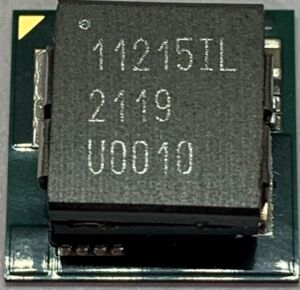
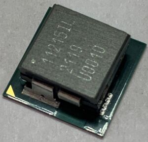
MPT11215il power module, wide Input Voltage RANGE, 15A buck converter with integrated inductor
STEP-DOWN DC-DC SWITCHING CONVERTER
mpt11215il: wide Input Voltage, 15A Power Module |
technical documentation |
|---|---|
 |
DATASHEET:  APPLICATION NOTE: APPLICATION NOTE: |
ordering information |
MoDULE FORM FACTOR |
||||||||||||||||
|---|---|---|---|---|---|---|---|---|---|---|---|---|---|---|---|---|---|
|
|
Features
- Excellent Ripple and Transient Performance
- Up to 15A Continuous Operating Current
- Wide 4.5V to 16V VIN range
- 0.6V to 5V VOUT range
- Optimized Solution Size
- Programmable switching frequency range from 550kHz to 1.2MHz
- Easy compensation with a single resistor
- Thermal, Over-Current, Short Circuit, Under-Voltage, and Pre-Bias Protections
- Pb-Free and RoHS Compliant, MSL Level 3, 260°C Reflow
Applications
- FPGAs, ASICs, DSPs, Network processors, Industrial applications
- High density double data rate (DDR) memory VDDQ rails
- Server Power Systems
- High Thermal requirement applications
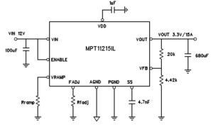
Pin Functions
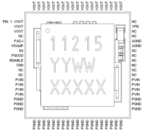
Figure 2: Pin Diagram (Top View)
NOTE A: NC pins are not to be electrically connected to each other or to any external signal, ground or voltage. However, they must be soldered to the PCB. Failure to follow this guideline may result in part malfunction or damage.
NOTE B: White ‘dot’ on top left is pin 1 indicator on top of the device package.
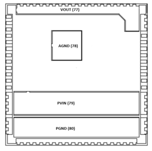
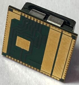
Figure 2A: Pin Diagram (Bottom View)
Pin Descriptions
| PIN | NAME | FUNCTION |
| 4, 11, 12 ,46-51,
54, 55, 57 |
NC | No Connect. These pins must be soldered to PCB but not electrically connected to each other or to any external signal, voltage, or ground. These pins may be connected internally. Failure to follow this guideline may result in device damage. |
| 1 – 3, 58 – 76, 77 | VOUT | Regulated converter output. Connect to the load and place output filter capacitor(s) between these pins and GND pins. Refer to the Layout Recommendation section for more details. |
| 17 – 41, 80 | PGND | Input/Output power ground. Connect to the ground electrode of the input and output filter capacitors. Refer to the Layout Recommendation section for more details. |
| 52, 53, 78 | AGND | Analog ground. Connect to system ground plane. Refer to the Layout Recommendation section for more details. |
| 13 – 16, 42 – 45, 79 | PVIN | Input power supply. Connect to input power supply. Decouple with input capacitor to GND pin. Refer to the Layout Recommendation section for more details. |
| 6 | VRAMP | Connect a resistor between VRAMP pin and GND to set the compensation. |
| 5 | FADJ | Frequency adjust pin. Connect a resistor between FADJ pin and
GND to set the switching frequency. Frequency can be programmed from 550KHz to 1.2MHz. |
| 7 | SS | Soft start control input pin. This pin is used to program the soft start
period with an external capacitor connected to GND. |
| 8 | PGOOD | Power good indication pin. It’s an open drain output. It will pull low when over current, short circuit, over temperature, UVLO, UVP, and output voltage loss of regulation, including output pre–bias. |
| 9 | ENABLE | Enable pin. Applying logic high to the ENABLE pin will enable the device and initiate a soft-start. Applying logic low disables the output and switching stops. ENABLE can be connected to VIN directly or through a resistor. There’s an internal 2uA pull up current source. |
| 10 | VDD | Internal 5.45V LDO output. Connect a 1uF capacitor from VDD to GND. |
| 56 | VFB | External feedback input pin. Connect a resistor between VFB and GND, and another resistor between VFB to VOUT to set the output voltage. Refer to the Output Voltage Setting section for more details. |
Electrical Characteristics
NOTE: VIN = 12V, Minimum and Maximum values are over operating ambient temperature, vin, and load range unless otherwise noted. Typical values are at Ta = 25°C.
| PARAMETER | SYMBOL | TEST CONDITIONS | MIN | TYP | MAX | UNITS |
| Operating Input Voltage (1) | PVIN | 4.5 | 16.0 | V | ||
| Under Voltage Lock-Out – VIN Rising | VUVLOR | Voltage above which UVLO is not asserted | 4.1 | 4.3 | 4.5 | V |
| Under Voltage Lock-Out – VIN Falling | VUVLOF | Voltage below which UVLO is asserted | 3.3 | V | ||
| Under Voltage Lock-Out Hysteresis | VUVLOHYS | 1 | V | |||
| Vout Over Voltage Protection | VOVPR | VFB rising | 117 | % | ||
| OVP Hysteresis | VOVP-HYST | VFB falling | 2.5 | % | ||
| Vout Under Voltage Protection | VUVPF | VFB falling | 94 | % | ||
| UVP Hysteresis | VUVP-HYST | VFB Rising | 3 | % | ||
| Shut-Down Supply Current | IS | ENABLE = 0V | 10 | mA | ||
| No Load Quiescent Current | IVINQ | VOUT = 1.2V | 4.5 | mA | ||
| Internal LDO output | VDD | 25mA load, Ta from -40℃ to 85℃ | 5.35 | 5.45 | 5.55 | V |
| Feedback Pin Voltage (2) | VFB | VOUT = 0.6V, ILOAD = 0, Ta =25°C | 0.594 | 0.6 | 0.606 | V |
| Feedback Pin Voltage (Line, Load, Temp.) | VFB | 4.5V ≤ PVIN ≤ 16.0V
0A ≤ ILOAD ≤ 15A ; -40°C ≤ Ta ≤ 85°C |
0.588 | 0.6 | 0.612 | V |
| Feedback pin Input Leakage Current (3) | IFB | VFB pin input leakage current | -50 | 50 | nA | |
| Soft start source current | ISS | SS=0V, Ta from -40℃ to 85℃ | 3 | 4 | 5 | mA |
| Soft start pulldown resistance | RSS | SS=0.8V | 80 | Ω | ||
| VOUT Rise Time (3) | tRISE | 1 | ms | |||
| Continuous Output Current | IOUT | 0 | 15 | A | ||
| Current Limit Trip Level | IOCP | VIN = 12V, VOUT = 1.2V, Ta from -40℃ to 85℃ | 25 | A | ||
| Current Limit Retry Time (3) | TCL_TRY | 2.5 | ms | |||
| Disable Threshold | VDISABLE | ENABLE pin logic going low | 1.1 | V | ||
| Enable Threshold | VEN | ENABLE pin logic going high | 1.18 | 1.2 | 1.4 | V |
| Enable Hysteresis | ENHYS | 100 | mV | |||
| Enable Internal Pullup Current | IEN | EN = 0V | 2 | mA | ||
| PGOOD pulldown resistance | RPG | PGOOD=0.1V | 100 | Ω | ||
| Switching Frequency | FSW | Programmable Switching frequency | 550 | 1200 | kHz |
(1) Minimum Vin voltage must be at least 1.3V higher than Vout.
(2) The FB pin is a sensitive node. Do not touch FB while the device is in regulation.
(3) Parameter not production tested but is guaranteed by design.
Layout Recommendations
Recommendation 1: Input and output filter capacitors should be placed on the same side of the PCB, and as close to the MPT11215IL package as possible. They should be connected to the device with very short and wide traces. Do not use thermal reliefs or spokes when connecting the capacitor pads to the respective nodes. The Input/Output Voltage and PGND traces between the capacitors and the MPT11215IL should be as close to each other as possible so that the gap between the two nodes is minimized, even under the capacitors.
Recommendation 2: In order to minimize the Power GND loop, it is recommended to route the input and output loops close to the same point, which is the ground of the MPT11215IL. Decoupling ceramic capacitors are to be placed as close as possible to the module in order to contain the switching noise in the smallest possible loops and to improve PVIN decoupling by minimizing the series parasitic inductance of the PVIN traces.
Recommendation 3: The large power thermal pads underneath the device must be connected to their respective planes through as many vias as possible. The drill diameter of the vias should be 0.33mm, and the vias must have at least 1-oz. copper plating on the inside wall, making the finished hole size around 0.2mm to 0.26mm. Do not use thermal reliefs or spokes to connect the vias to the ground plane. This connection provides the path for heat dissipation from the converter.
Recommendation 4: Multiple small vias (the same size as the thermal vias discussed in recommendation 3 should be used to connect ground terminal of the input capacitor and output capacitors to the system ground plane. Put the vias under the capacitors along the edge of the GND copper closest to the Voltage copper. These vias connect the input/output filter capacitors to the GND plane, and help reduce parasitic inductance in the input and output current loops. If the vias cannot be placed under CIN and COUT, then put them just outside the capacitors along the GND slit separating the two components. Do not use thermal reliefs or spokes to connect these vias to the ground plane.
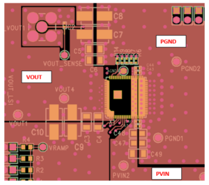
Figure 8: Illustration of Layout recommendations 1 to 4.
Recommendation 5: It is recommended that below the MPT11215IL module, the layers under the top layer should be solid ground planes. This will provide good shielding and lower the ground impedance at the top layer where the module is mounted. AGND should also be routed as a copper plane, in order to reduce the ground impedance.
Recommendation 6: It is highly recommended to use separate nets for AGND and PGND and connect them through a 0Ω resistor or a short. This will help prevent noise from the noiser Power Ground disturbing the more sensitive Analog Ground. The PGND connection point should be near the Output Capacitor GND termination as that GND point is not as noisy as the Input capacitor GND points.
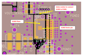
Figure 9: Illustration of Layout recommendations 6.
Package drawings
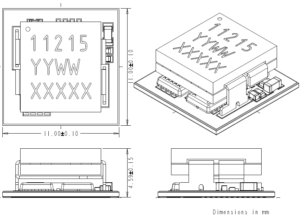
Figure 10: Open Frame Package Drawing