MPT11203IQ POWER MODULE, HIGH INPUT VOLTAGE, 3A BUCK CONVERTER WITH INTEGRATED INDUCTOR
STEP-DOWN DC-DC SWITCHING CONVERTERS
mpt11203iq: MPT High Input Voltage, 3A Power Module |
technical documentation |
|---|---|
 |
DATASHEET: |

ordering information |
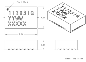
MoDULE FORM FACTOR |
||||||||||||
|---|---|---|---|---|---|---|---|---|---|---|---|---|---|
|
 |
Features
- Excellent Ripple (<2mV) and Transient Performance
- Up to 3A Continuous Operating Current
- Up to 16V Input Voltage Range
- 5% Vfb Initial Accuracy
- 890kHz Switching Frequency
- Optimized Solution Size
- Thermal, Over-Current, Short Circuit, Under-Voltage and Pre-Bias Protections
- 455µA Low Quiescent Current
- Pb-Free and RoHS Compliant, MSL Level 3, 260°C Reflow
Applications
- Point of Load Conversion for 7V – 16V input rail
- Space constrained and noise sensitive applications
- High Thermal requirement applications
- Storage (SSD, HDD), Embedded, LV I/O System Power
- FPGAs, ASICs, DSPs, Network processors, Industrial applications
- Security Cameras, Test and Measurement, Portable devices, Medical devices
Pin Functions
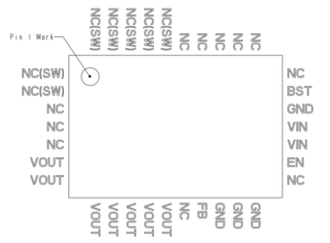
Figure 2: Pin Diagram (Top View)
NOTE A: NC pins are not to be electrically connected to each other or to any external signal, ground or voltage. However, they must be soldered to the PCB. Failure to follow this guideline may result in part malfunction or damage.
NOTE B: White ‘dot’ on top left is pin 1 indicator on top of the device package.
Pin Descriptions
| PIN | NAME | FUNCTION |
| 1, 2, 30, 31, 32, 33, 34 | NC(SW) | No Connect. These pins are internally connected to the common switching node of the internal MOSFETs. They must be soldered to PCB but not be electrically connected to any external signal, ground, or voltage. Failure to follow this guideline may result in device damage. |
| 3, 4, 5,13,18,24,25 26,27,28,29 | NC | No Connect. These pins must be soldered to PCB but not electrically connected to each other or to any external signal, voltage, or ground. These pins may be connected internally. Failure to follow this guideline may result in device damage. |
| 6, 7, 8, 9,10,11,12 | VOUT | Regulated converter output. Connect to the load and place output filter capacitor(s) between these pins and GND pins. Refer to the Layout Recommendation section. |
| 15,16,17,22 | GND | Input/Output power ground. Connect to the ground electrode of the input and output filter capacitors. See VOUT and VIN pin descriptions for more details. |
| 20, 21 | VIN | Input power supply. Connect to input power supply. Decouple with input capacitor to GND pin. Refer to the Layout Recommendation section. |
| 19 | EN | Enable pin. Applying logic high to the EN pin will enable the device and initiate a soft-start. Applying logic low disables the output and switching stops. EN can be connected to VIN directly or through a resistor. |
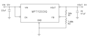
| 14 | FB | External feedback input pin. Connect resistor between FB and GND, and another resistor between FB to VOUT to set the output voltage. Refer to Output Voltage Setting in page 15 for a description of resistor selection. |
| 23 | NC(BST) | Bootstrap pin. This pin is internally connected to a capacitor to SW to form a floating supply across the high-side switch driver. This pin must be soldered to PCB but not be electrically connected to any external signal, ground, or voltage. Failure to follow this guideline may result in device damage. |
Electrical Characteristics
NOTE: VIN = 12V, Minimum and Maximum values are over operating ambient temperature, vin, and load range unless otherwise noted. Typical values are at TA = TJ = 25°C.
| PARAMETER | SYMBOL | TEST CONDITIONS | MIN | TYP | MAX | UNITS |
| Operating Input Voltage (1) | VIN | 7 | 16 | V | ||
| Under Voltage Lock-Out – VIN Rising | VUVLOR | Voltage above which UVLO is not asserted | 4.1 | 4.13 | 4.22 | V |
| Under Voltage Lock-Out – VIN Falling | VUVLOF | Voltage below which UVLO is asserted | 3.8 | 3.93 | 4.05 | V |
| Under Voltage Lock-Out Hysteresis | VUVLOHYS | 200 | mV | |||
| Shut-Down Supply Current | IS | EN = 0V | 10 | mA | ||
| No Load Quiescent Current | IVINQ | VOUT = 1.2V | 210 | 455 | 895 | mA |
| Feedback Pin Voltage (2) | VFB | VOUT = 0.6V, ILOAD = 0, TA =25°C | 0.596 | 0.605 | 0.614 | V |
| Feedback Pin Voltage (Line, Load, Temp.) | VFB | 7V ≤ VIN ≤ 16V
0A ≤ ILOAD ≤ 3A ; -40°C ≤ TA ≤ 85°C |
0.590 | 0.605 | 0.620 | V |
| Feedback pin Input Leakage Current (3) | IFB | VFB pin input leakage current | 18 | 60 | nA | |
| VOUT Rise Time (3) | tRISE | 0.8 | 1.5 | ms | ||
| Continuous Output Current | IOUT | 0 | 3 | A | ||
| Valley Current Limit Trip Level | IOCP | VIN = 12V, VOUT = 1.2V | 4.2 | 4.5 | A | |
| Current Limit Retry Time (3) | TCL_TRY | 2.5 | ms | |||
| Disable Threshold | VDISABLE | EN pin logic going low | 1.05 | V | ||
| Enable Threshold | VEN | EN pin logic going high | 1.1 | 1.2 | 1.4 | V |
| EN Hysteresis | ENHYS | 150 | mV | |||
| EN Pin Input Current | IEN | EN = 2.0V | 1.5 | 2 | mA | |
| Switching Frequency | FSW | Free running frequency of oscillator | 890 | kHz |
(1) Minimum Vin voltage must be at least 1.3V higher than Vout.
(2) The FB pin is a sensitive node. Do not touch FB while the device is in regulation.
(3) Parameter not production tested but is guaranteed by design.
Layout Recommendations
Recommendation 1: Input and output filter capacitors should be placed on the same side of the PCB, and as close to the MPT11203IQ package as possible. They should be connected to the device with very short and wide traces. Do not use thermal reliefs or spokes when connecting the capacitor pads to the respective nodes. The Voltage and GND traces between the capacitors and the MPT11203IQ should be as close to each other as possible so that the gap between the two nodes is minimized, even under the capacitors.
Recommendation 2: Half of the PGND pins are dedicated to the input circuit and the other half to the output circuit. Incorporting a slit separating the input and output GND circuits helps minimize noise coupling between the converter input and output switching loops.
Recommendation 3: The system ground plane should be on the 2nd layer (below the surface layer). This ground plane should be continuous and un-interrupted.
Recommendation 4: The large thermal pad underneath the device must be connected to the system ground plane through as many vias as possible. The drill diameter of the vias should be 0.33mm, and the vias must have at least 1-oz. copper plating on the inside wall, making the finished hole size around 0.2mm to 0.26mm. Do not use thermal reliefs or spokes to connect the vias to the ground plane. This connection provides the path for heat dissipation from the converter.
Recommendation 5: Multiple small vias (the same size as the thermal vias discussed in recommendation 4 should be used to connect ground terminal of the input capacitor and output capacitors to the system ground plane. Put the vias under the capacitors along the edge of the GND copper closest to the Voltage copper. These vias connect the input/output filter capacitors to the GND plane, and help reduce parasitic inductance in the input and output current loops. If the vias cannot be placed under CIN and COUT, then put them just outside the capacitors along the GND slit separating the two components. Do not use thermal reliefs or spokes to connect these vias to the ground plane.
Recommendation 6: The VOUT sense point should be connected at the last output filter capacitor furthest from the VOUT pins. Keep the sense trace as short as possible in order to avoid noise coupling into the control loop.
Recommendation 7: As with any switch-mode DC-DC converter, try not to run sensitive signal or control lines underneath the converter package on other layers.
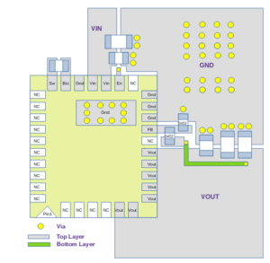
Figure 6: Recommended PCB Layout
Package drawings